Configure RSLinx to Talk to SLC
- Attach a null modem cable (or the A-B CP3 programming cable) from your PC serial port to the serial port on your SLC processor, called Channel 0.
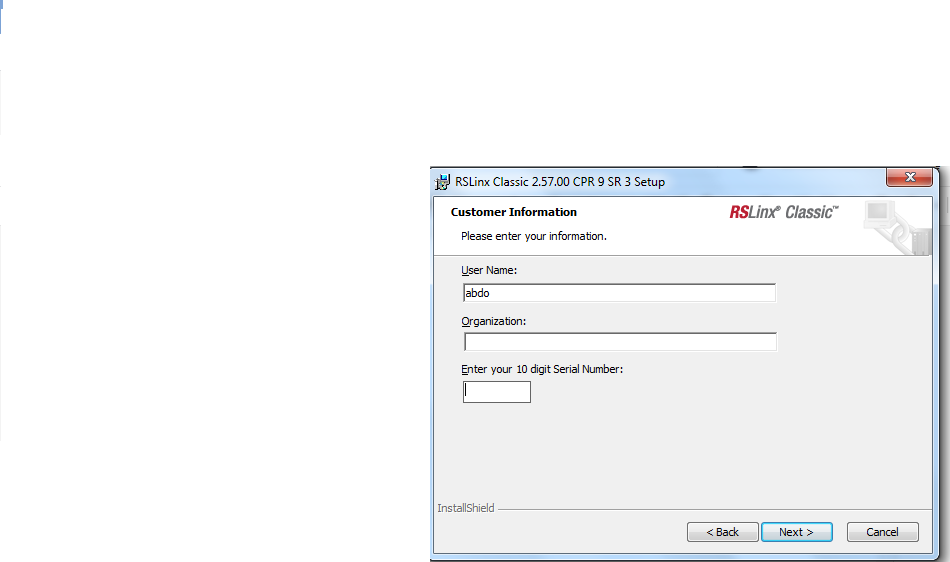
- Open RSLinx. Click on the Communicationsdrop-down menu. Click on the “Configure Drivers option. If you’re running a newer version of RSLinx, youâ see a dialog box like this one:
- If you already have a RS-232 DF-1 driver configured, skip to the Auto Configure instructions in Step 5.
- Click the down arrow in the “Available Driver Types: option box and click on “RS-232 DF-1 devices, as shown, and click the “Add New button.
You will now be prompted to name your driver. For most cases, the default name will be acceptable. To match the sample project used in this lab, accept the default name by clicking the button
- Next, you will see the driver setup dialog box.
- First, click the down arrow in the œComm Port option box and click the Comm port that matches the number on your PC (usually Comm1, Comm2, Comm3, or Comm4).Â
- Then, click the down arrow in the Devices: option box and click the SLC-CH0/Micro/PanelView option.Â
- Finally, click the “Auto Configure button. RSLinx will then query the processor, establish a communications link, and adjust the driver parameters to match the processorâs current port configuration. Don worry if the parameters in your driver don match the ones shown in the following example. As long as the window reports œAuto Configuration Successful!â€, whatever parameters appear for baud rate, parity, error checking, etc. will be correct. A successful result will look something like this:
In some instances, RSLinx will fail to Auto Configure. If this happens to you, first check that your cable is OK, properly connected, and that you are selecting the correct Comm port. Once this is verified, if Auto Configure fails, you will need to completely wipe the processor memory and reset it to factory defaults. Consult the A-B product documentation, the A-B website, or A-B Tech Support for instruction on how to do this. Once done, the RSLinx should be able to Auto Configure.
Clicking on will return you to this dialog:
Clicking on will return you to this dialog:
- If the driver status is “Runningâ€, you have now successfully configured RSLinx to talk to the processor. Click the “Close†button to close this dialog and then exit but do not shutdown RSLinx by clicking the “File†menu option and then “Exit and Shutdownâ€. Be sure to click the “Exit†option.
Use RSLogix500 to Modify the Sample Project
- Next, we will load and configure the sample ladder logic program and download it to the processor. Start RSLogix500. It should come up to a blank window, like this:
Click on the drop-down menu, click Open and browse to the folder where you saved the sample ladder and double-click the file, MVI46MCM.RSS is included on the MVI46MCM CD.
- This will open the sample project. We can now configure the sample ladder to get it ready for the next exercise.
- You get a window that looks like this. If not, then click on the ViewMenu, and make sure there are check marks beside “Standardâ€, “Onlineâ€, and “Tabbed Instruction Bar†options.
In the left pane Project Tree area, under the Controller folder, double-click on Configuration icon. This will display the I/O Configuration dialog box:
Click on OTHERin Slot 1, as shown, then click the
Configbutton.
Configbutton.
- Make sure the values are as shown. If they are not, set them to these values. Otherwise, the module will not function properly. Details on module setup are contained in the User’s Manual in Section 3.3 “Setting Up the Moduleâ€. After you verify the values, click “OK†or “Cancel†to close this dialog box. Click on the Exit icon () in the upper-right corner of the I/O Configuration dialog to close it and return to the main window.
- In the left pane Project Tree area, under the Data Files folder, double-click on the N10 – MCM CFG icon. Set the values in this file to match the ones shown below.
| MCM Ports 1 & 2 Cmds |
| Port 1 / Port 2 |
| - N10:10 / N10:40Â Port Enable/Disable |
| - N10:11 / N10:41Â Port Type |
| - N10:12 / N10:42Â Float Flag |
| - N10:13 / N10:43Â Float Start |
| - N10:14 / N10:44Â Float Offset |
| - N10:15 / N10:45Â Protocol |
| - N10:16 / N10:46Â Baud Rate |
| - N10:17 / N10:47Â Parity |
| - N10:18 / N10:48Â Data Bits |
| - N10:19 / N10:49Â Stop Bits |
| - N10:20 / N10:50Â RTS On Delay |
| - N10:21 / N10:51Â RTS Off Delay |
| - N10:22 / N10:52Â Min. Response Delay |
| - N10:23 / N10:53Â Use CTS Line |
| - N10:24 / N10:54Â Slave ID |
| - N10:25 / N10:55Â Bit Input Offset |
| - N10:26 / N10:56Â Word Input Offset |
| - N10:27 / N10:57Â Output Offset |
| - N10:28 / N10:58Â Holding Register Offset |
| - N10:29 / N10:59Â Command Count |
| - N10:30 / N10:60Â Min. Command Delay |
| - N10:31 / N10:61Â Command Error Pointer |
| - N10:32 / N10:62Â Response Timeout |
| - N10:33 / N10:63Â Retry Count |
| - N10:34 / N10:64Â Error Delay Count |
| - N10:35 / N10:65Â Reserved |
| - N10:36 / N10:66Â Guard Band |
| - N10:37 / N10:67Â Guard Band Timeout |
- This configuration data will set module Port1 to be a Modbus Master and Port2 to be a Modbus Slave. Both ports will be set for Modbus RTU mode, 57,600-baud, no parity, 8 data bits, 1 stop bit. Hardware handshaking will be disabled (RTS/CTS not used.) We will be able to use up to 5 Modbus Commands and any Modbus Command Errors will be sent to module memory beginning at register address 300, which will then appear in SLC data table N31, beginning at N31:100. With this configuration, we can use a second null modem
cable and two DB9M-to-RJ45 pigtails to connect the two ports together, which in turn will allow us to send and get data from the module with our sample ladder. Click on the Exit icon () in the upper-right corner of the Data File N10(dec) dialog to close it and return to the main window. - We will now configure our Modbus commands for Port1. In the left pane Project Tree area, under the Data Files folder, double-click on the N11 – P1 CMDS icon. Set the values in this file to match the ones shown below.
| MCM Ports 1 & 2 Cmds |
| Port 1 / Port 2 |
| - N11:0 / N12:0Â Cmd Enable |
| - N11:1 / N12:1Â Internal Address |
| - N11:2 / N12:2Â Poll Interval Time |
| - N11:3 / N12:3Â Count |
| - N11:4 / N12:4Â Swap Code |
| - N11:5 / N12:5Â Node Address Device ID |
| - N11:6 / N12:6Â Function Code |
| - N11:7 / N12:7Â Device Address Register |
- This creates one Modbus command for Port1, our Master port. This command will send a request out Port1 to the Modbus Slave at Slave ID 2 (our Port2), as configured in N10. The command will get twenty 16-bit words (registers) of data from Destination Address 0, our module address 0, the first word of our WRITE DATA area, and move it out Port2, in Port1, and store it in Internal Address 200, our module address 200, the first word of our READ DATA area. This command will execute once each second.  This way, any values we poke into data table addresses N32:0 through N32:19 will, after a short delay, appear in the corresponding addresses in data table N31. Click on the Exit icon () in the upper-right corner of the Data File N11 (dec) dialog to close it and return to the main window.
- In the left pane Project Tree area, under the Data Files folder, double-click on the N12 – P2 CMDS icon. Set all the values in this file to zero and click on the Exit icon () in the upper-right corner to close this window and return.
- In the left pane Project Tree area, under the Data Files folder, double-click on the N32 – WRITE DATA icon. Set the values in this file as shown
Downloading and Testing the Modified Sample Project
- Make sure your null modem cable (or CP3 programming cable) is still attached between your PC Comm port and the processor RS-232 port. Take the two DB9M-to-RJ45 pigtails and the other null modem cable and connect the lower two ports on the MVI46MCM module,
P2 APPLICATION and P3 APPLICATION, with these cables. - Set the processor key switch to thePROGposition. In RSLogix500, click the down-arrow next to the “OFFLINE†status and click “Download…†from the menu.
When you see the confirmation dialog, click the Yesâ button.
The sample ladder is currently configured for a 1747-L551 SLC 5/05. If you are using a different processor, when you try to download, you will see the following:
If you get this warning screen, click the “OK button. RSLogix will automatically determine the actual processor type you are using and adjust the IO Configuration to match your installed processor. You should then see the following window:
When it comes up, make sure the “Clear I/O†box is NOT checked, as shown, and click “OKâ€. A Download Progress dialog will flash through several progress bars as various parts of the program are loaded. Eventually, you should see:
Click the “Yes†button. The RSLogix status box will change to show you are on-line live with the processor. You can also tell you are on-line when you see the colored blocks and ladder rotating in the status box. The faster they rotate, the higher your connection speed. It should look like this (with animated ladder):
- If you had to change your processor type, now would be a good time to re-save the program.
- Next, we will change the SLC 500 processor key switch from œPROG to “RUN†and back to theREM position. If you have a good program, the processor RUN LED will light up solid green and, on the MVI46MCM module, the OK LED will change from red to green, the APP STATUS and BP ACT LEDs will be amber and the LEDs for P2 and P3 will flash green about once every second. The RSLogix status box should look like this:
If, however, the processor “FAULT†LED flashes red and you see this,
it indicates some kind of hardware or software problem. Common causes include: hardware failure, ladder logic errors, and installing the MVI46MCM module in a different chassis slot than the one selected in the I/O Configuration, I/O modules in the configuration that are not actually installed in the chassis, and more. Assuming you are still on-line with the processor, to see what might be causing the problem, you can check the “Processor Status†dialog for the Major Error Code causing the fault. In the Project Tree, under the
“Controller†folder, click on “Processor Status†then click on the “Errors†tab to see the fault. An example of having the module in the wrong slot is shown. Your error may be different.
“Controller†folder, click on “Processor Status†then click on the “Errors†tab to see the fault. An example of having the module in the wrong slot is shown. Your error may be different.
- Do whatever is required to fix the root cause of the fault and then turn the key switch from “REM†to œPROG†to RUN and back to œREM to get the processor running normally.
- NOWâWeâre ready for some real fun. Take a few minutes to look at the three LAD files in our test program. For a detailed explanation of what these files do, look at Chapter 4 – Ladder Logic in the User’s Manual, beginning on page 25.
Now, look in LAD 4 MCM CMDS at rungs 0002 and 0003. Bit B3:0/0 in rung 0002 is called the Cold Boot bit. Bit B3:0/1 in rung 0003 is called the Warm Boot bit. Either may be toggled to force the module to restart, reload its configuration and any Modbus commands. This is a handy feature that makes it easy to change and test different configurations and commands. Itâ quicker and safer to toggle these bits than to recycle the processor or power-down and power-up the chassis to accomplish the same thing. Toggling either of these bits allows configuration and command changes to be performed without halting the processor. This can be very useful when added one of our modules to an existing application already in use at a customer site. As we progress through the rest of this exercise, we will be returning to this ladder and these rungs often as we modify and test our program.
Toggle one of these bits now and watch the LEDs on the front of the module as you do so. You should see the P2 and P3 LEDs stop the regular blinking they had been doing, the OK LED will briefly turn red then go back to green, and then the P2 and P3 LEDs should resume their blinking once a second.
To toggle the bit, right-click on its picture then click onœToggle Bit†at the bottom of the context menu, as shown. Be sure to watch the face of the MVI46-MCM module as you click.
Now we can check to be sure our program is moving the data as it should. Remember previously that we zeroed out our READ DATA table and put test values in our WRITE DATA table. If our program is working correctly, we should now have the same values in the same relative addresses in our READ DATA as in the WRITE DATA. First, letâs check the WRITE DATA table to be sure our test values are still there. In the Project Tree, under the Data Files folder, double-click “N32 WRITE DATAâ€.